
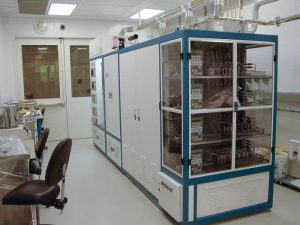
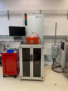
TL01 Tystar LPCVD Furnace
Process Data
Process Data T1: Silicon-Nitride
Process Data T1: Low-Stress Nitride
Process Data T3: N+ PolySilicon
Process Data T3: P+ PolySilicon
Process Data: Low-Temperature Oxide
Control Charts
Control Chart: Silicon Nitride
Control Chart: Low-Stress Nitride
Control Chart: Low-Temperature Oxide
PM Details
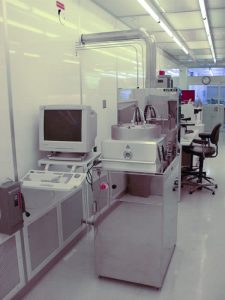
PD01/ PD02 Plasma-Therm 790 PECVD
PD01 is a Plasma-Therm 790 PECVD tool that is configured with 2% silane in helium to deposit high-quality silicon dioxide, silicon nitride, and amorphous silicon films at temperatures from 100 C to 300 C. The tool was donated to UTD in May 2004 by the Mykrolis Corporation. PD02 is also a Plasma-Therm 790 PECVD system that can deposit high quality silicon carbide, silicon oxide, silicon nitride films. The tool was purchased for the lab by Dr. Stuart Cogan in Fall 2013.
Process Data
Control Charts
TC02 Ultratech/Cambridge NanoTech Savannah 100 Atomic Layer Deposition
The Atomic Layer Deposition system deposits thin films of dielectrics such as hafnium oxide, silicon oxide, and aluminum oxide. The tool can be configured for titanium oxide upon user request. The tool can easily switch from water to ozone precursor. Users may request additional training on the ozone generator.
Process Data
Process Data: 10nm HfO2 with H2O
Process Data: 10nm HfO2 with O3
Control Chart
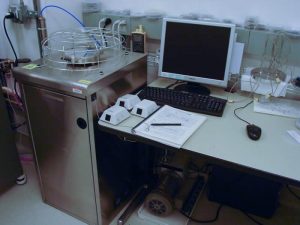
TD03 SCS Parylene Deposition
The Parylene coater deposits parylene in thin films to serve as an insulating coating for organic semiconductors.
PD03 Plasma-Therm Vision 310 PECVD
PD03 is a PlasmaTherm Vision 310 plasma enhanced chemical vapor deposition (PECVD) instrument in service since 2021. It deposits high-quality silicon oxide of uniform thickness across the whole sample platen at 300 degree C deposition temperature. It also supports silicon carbide films deposition using various custom recipes developed at UT Dallas.
TC03 PICOSUN R-200 Advanced Plasma ALD–COMING Fall 2020
For metal and metal nitride deposition…coming fall 2020