
HMDS Process
2-21-03
By Joe Daggett (Texas Instruments, DMOS 6)
Dr. Samuel Villareal (UT Dallas, IC Manufacturing Professor)
Dr. Roger Robbins (UT Dallas, Clean Room Manager, Provost Office) John Goodnight, (UT Dallas, Technical Staff Associate)

Abstract
The University of Texas at Dallas’, Erik Jonsson School of Engineering and Computer Science, has a semiconductor integrated circuit fabrication laboratory used for training students in semiconductor manufacturing, as well as, research for various IC and MEMS projects. For these training activities and research projects various types of microlithography are employed. Historically, the laboratory used spin-on HMDS as an adhesion promoter for the photoresist used for the microlithography. As part of a senior project an HMDS vapor prime process was setup. This process provides a safer, less expensive and superior process than the existing spin-on HMDS process. This paper will outline the YES-310 HMDS Vapor Prime Oven process, the experimentation used to set up the process, and the validation data for the process.
Introduction: HMDS Process
As a photoresist adhesion promoter for semiconductor applications, hexamethyldisilizane (HMDS) was first described in U.S. Patent 3,549,368 by R. H. Collins and F. T. Devers (1970) of IBM. Initially, processes called for 100% HMDS or HMDS mixed with Xylene. Wafers were dipped in the solution or the solution was dispensed onto a wafer using resist-processing equipment (Elliot 121-2). The first vapor prime techniques used bubblers or vapor degreasers with a reserve of liquid HMDS (VanZant 184). Vapor prime subsequently became the preferred technique for several reasons. 1) It allows for reduced chemical consumption and less wafer contamination (184-5). 2) It provides adhesion longevity even in the presence of high relative humidity (Y.E.S.). 3) Vacuum prime offers the advantage of combined dehydration and priming in the same process chamber.
HMDS priming has become a well-understood process, which can be chemically stable for several weeks (Y.E.S.). This photoresist adhesion enhancement process is effective and is a standard semiconductor industry technique.
For several years, statistically designed experiments (DOE’s) have been performed on many aspects of the lithography process including the HMDS process. The DOE’s for the HMDS process all show good agreement with each other on the effects of dehydration bake, dispense time, dispense flow rate, and chemical reaction time. This paper introduces the HMDS process, summarizes the results from several statistically designed experiments (DOE’s), makes recommendations for the process and shows validation data of the process derived for the laboratory.
HMDS Process
As part of the semiconductor manufacturing process, photolithography is used to delineate patterns representing particular device or circuit structures on the surface of a silicon wafer. This pattern is made with photoresist, which protects the substrate underneath it from subsequent processing. The physical or electrical characteristics of the unprotected surfaces are altered by the following process steps such as etch, deposition, ion implantation, sputtering, etc. This cycle is repeated many times until the entire device is completed as depicted in figure 1.
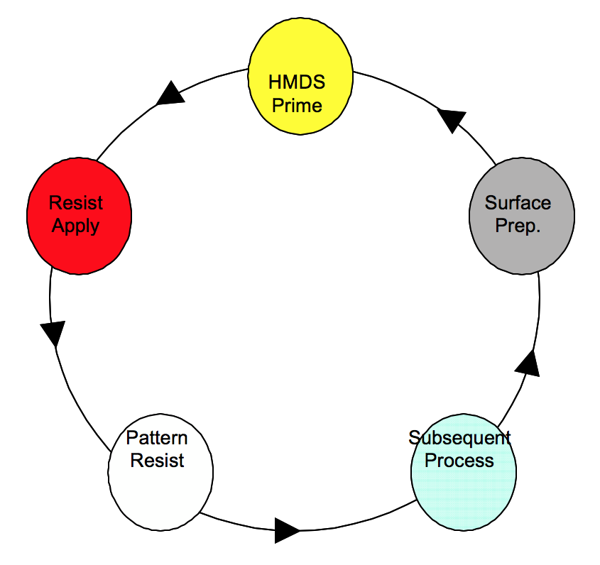
Figure 1. Repeated steps for manufacturing Integrated Circuits.
Good adhesion of the photoresist is important to ensure the integrity of pattern/electrical characteristic transfer. However, photoresist will not adhere to a hydrated silicon surface, so the silicon surface of the wafer must be dehydrated. Additionally, to further prepare the silicon surface for superior adhesion of the photoresist, a priming process using hexamethyldisilizane (HMDS) is performed. These requirements make the HMDS process a two step chemical reaction, dehydration and HMDS reaction.
Elevating the temperature of the wafer and reducing the pressure are used to accomplish dehydration of the wafer surface. The reduction in pressure lowers the boiling point of water to improve the dehydration induced by the elevated temperature. A vacuum venturi is used to generate the lower pressure in the reaction chamber and the bottom of the chamber is a hotplate that elevates the temperature of the wafer. While this process may not totally eliminate all of the water on the surface of the wafer, particularly the chemically bound water, it does remove a large percentage. The wafer is now ready for the HMDS reaction portion of the process.
During the HMDS reaction, the process chamber is flooded with HMDS vapor using nitrogen as a carrier gas. The HMDS ties up the molecular water on a hydroxylated silicon dioxide surface with a portion of the complex molecule and bonds the ends of the photoresist molecule with the other portion of the HMDS molecule. Thus, the twin-ended molecular bonding mechanism makes HMDS an excellent surface-linking adhesion promoter (Elliot, 120). This reaction is schematically represented in figure 2.
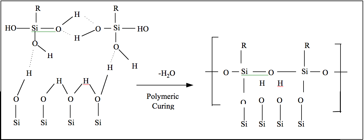
Figure 2. HMDS Chemical Reaction.
The result of the dehydration bake and HMDS prime is that the wafer becomes hydrophobic. Hydrophobisity can be measured using the contact angle of water to the hydrophobic surface (Bergh, Nistler).
Contact angle data is collected by placing a droplet of deionized water on the surface and by measuring the angle at the interface of the water and the silicon surface using a goniometer or optical comparator. According to the Young model (Frieser), (Figure 3), a droplet of water at rest upon a surface assumes a shape controlled by three forces of interfacial tension, γL cos θ = γS – γSL, where γS represents dispersive forces including gravity and adhesion properties of the two materials, γSL is dispersive force of DI water’s own cohesive properties, γL is the surface tension of the DI water. and, θ is the contact angle of interest to us.
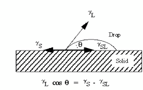
Figure 3. Young’s Model. In this equation θ is the contact angle between the liquid and solid.
The hydrophobicity is also affected by various parameters such as temperature, pressure, time, and chemical density. Experimentation has shown that temperature and pressure do not have a large affect on the chemical reaction and that time has a large affect on the chemical reaction (Daggett, Markowski, Preston). In these tests mathematical models are derived from statistically designed experiments. These models allow the optimization of the process, as well as, aid in troubleshooting any variation in the process results. Best microlithography results are obtained with contact angles between 65° and 80°.
Measurement and Analysis
Contact Angles: Figure 4 shows a Ramé-Hart, Inc., NRL Contact Angle Goniometer, Model
100-00-(115) was used to measure the contact angle data. All data was collected on 200mm virgin silicon wafers using 5µL of de-ionized water. The typical accuracy of a goniometer is ±2° (Nistler). The wafers were oriented during processing with the notch facing the operator. Figure 5 shows the measurement pattern, and figure 6 shows what the measurements look like with and without HMDS.
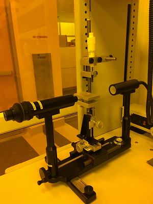
Figure 4, Ramé-Hart, Inc., NRL Contact Angle Goniometer, Model 100-00-(115).
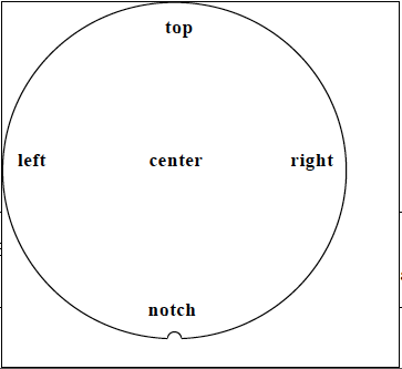
Figure 5. Goniometer Measurement Sites.
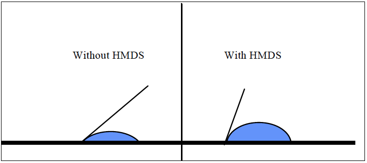
Figure 6, Representation of Goniometer Readings With and Without HMDS.
Experimentation
In an effort to characterize the HMDS process, the following screening design of experiment data was collected from Markowski historic data, (in the same model oven) and experiments run in the UT Dallas clean room. Table 1 lists the parameters tested to model the HMDS process.
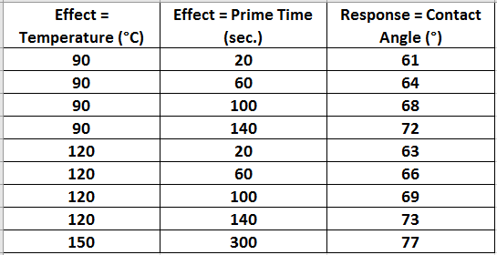
Table 1 HMDS Characterization DOE parameters.
SAS Institute JMP 4.0 software was used to model the process results collected. The first section below shows the fit of the model to the actual data. The data is plotted for a visual interpretation followed by tables that summarize the mathematical fit, (Figure 7). In the plot the solid line is the predicted value, and the dashed lines are the range of the predicted value with a
95% confidence interval. As can be see, the model corresponds well with the actual data showing an R square value over 98%. The R square is high for a typical model but not surprising since the process is a simple. The remaining variance not explained by the model can easily be explained by the repeatability of the measurement tool, which is ±2.0°.
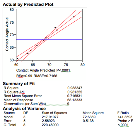
Figure 7. HMDS Model.
This next section models the effects each parameter has on the response (contact angles). The Effects Test, Table 2, numerically shows that Prime Time is the largest effect on contact angle followed by the interaction of Temperature*Prime Time, and lastly Temperature. These effects are graphically depicted in figures 8, 9, and 10 respectively.
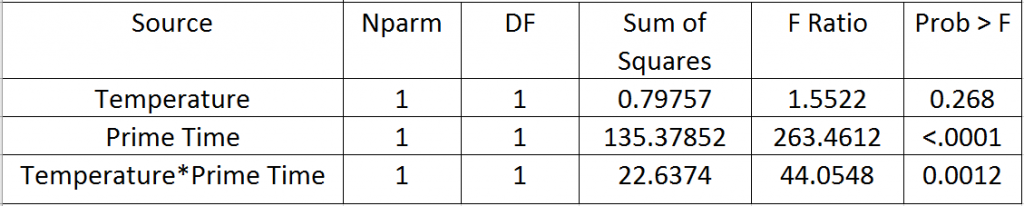
Table 2
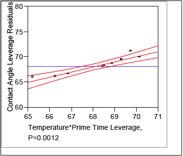
Figure 9. Temperature*Prime Time Leverage.
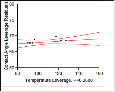
Figure 10. Temperature Leverage.
Finally, using the model, prediction of process results can be made. The Prediction Profiler below shows the parameters used to achieve the maximum contact angle in the HMDS vapor over.
Specifically, a Temperature of 150°C and a Prime Time of 300 seconds were used. One observation needs to be explained. The slope of the predicted contact angle as a function of temperature is negative. This observation leads one to believe that higher contact angles can be achieved at lower temperatures. This observation was investigated in the model which showed that the slope of contact angles versus temperature inverted at a prime time of ~122 seconds. This corresponded to the boiling/decomposition temperature of HMDS. One might ask why we bake at such a high temperature. The explanation is determined by the goals of the process. As mentioned above the first goal is to dehydrate the substrate surface. So the answer is to optimize both the dehydration and the contact angle. As shown in the Prediction Profiler, (Figure 11), a contact angle of 77.3 is predicted as a result of the process parameters.
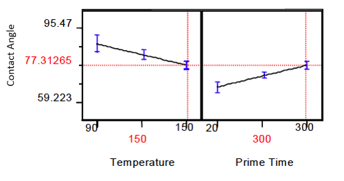
Figure 11. Prediction Profiler.
Process Test
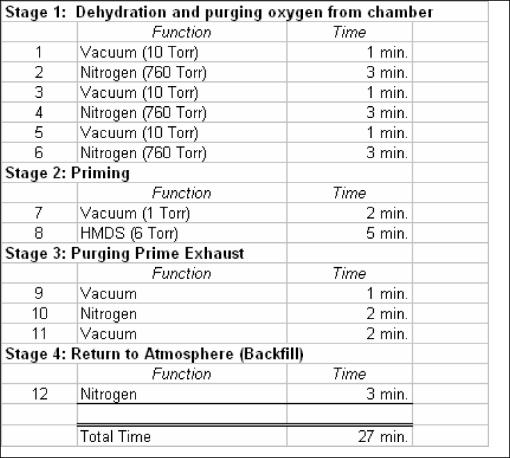
Table 3. Y.E.S. Process Recipe. The table below lists the recipe used on the vapor prime oven. The recipe is the manufactures recommended process.
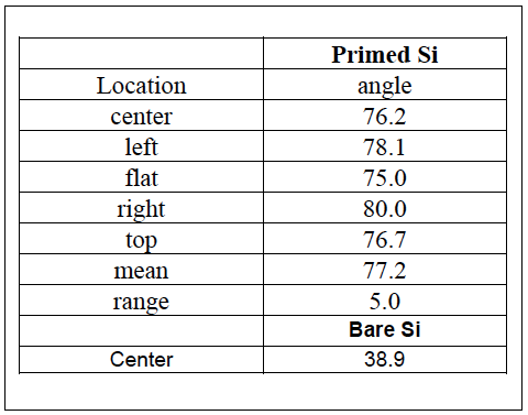
The table below shows the process results obtained using the recipe listed above. Excellent agreement is achieved between actual and modeled results. Also included in the table is the contact angle measured on a bare silicon wafer as a reference for the process.
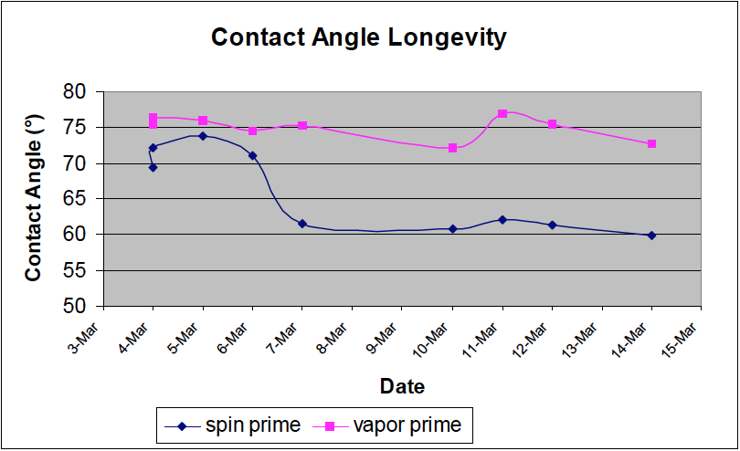
This last plot shows a longevity study performed on the process comparing a spin-on primed wafer and a vapor primed wafer. This shows stable contact angles on the vapor primed wafer at least two weeks while the spin-on primed wafer’s contact angles degrade below the recommended contact angle after three days. Variation in the data can be attributed to measurement repeatability and process uniformity.
Conclusions
HMDS is flammable and spin-on priming in the UT Dallas laboratory is performed by hand dispensing ~5ml of HMDS onto a wafer via pipette and spinning the wafer until it dries. This exposes the human to a potential fire hazard. Further, HMDS is a carcinogen and exposure should be avoided. In the YES LPIII oven, the user is not exposed to the HMDS vapors, less than 1ml is used to prime up to 200 wafers. Vapor prime is therefore safer, less expensive and as shown in experimentation achieves better contact angles that last longer.
Appendix A – Work Cited
Bergh, A.A., The Correlation between Water Contact Angle and KPR Adherence on SiO2 Surfaces, Journal of Electrochemical Society, Vol. 112, No. 4., April 1965.
Box, George E.P., et al. Statistics for Experimenters, New York, John Wiley & Sons, 1978
Daggett, Joe. et al., POLARIS 2100/2200 Cluster Vapor Prime Process Optimization Based on a Five-Factorial Design of Experiments, FSI International, Document No. 1066-TRM-0897, August 1997.
Elliot, David J., INTEGRATED CIRCUIT FABRICATION TECHNOLOGY, New York, McGraw-Hill, 1982 Frieser, R. G., Characterization of Thermally Grown SiO2 Surfaces by Contact Angle Measurements. Journal of the Electrochemical Society, Vol. 121, No. 5, May 1974.
Markowski, Mark S., VAPOR PRIMING OPTIMIZATION USING CONTACT ANGLE MEASUREMENTS, Shipley Company, Technical Paper, February 1999.
Nistler, John L., A SIMPLE TECHNIQUE TO ANALYZE CONDITIONS THAT AFFECT SUBMICRON PHOTORESIST ADHESION, KTI Microelectronics Seminar Interface ‘88 Proceedings, page 233, November 10, 1988.
Preston, Steve. Improving Contact Angles with HMDS Prime Process. FSI International, Document No. 1017-TRM-1196, Oct. 21, 1996.
Rame-Hart. A Bibliography of Contact Angle Use in Surface Science. Rama-Hart, Inc. Technical Bulletin TB-100
SAS Institute Inc. JMP Version 4.0. 1989
Y.E.S., LP2 (product bulletin), Yield Engineering Systems.
Van Zant, Peter. MICROCHIP FABRICATION, A PRACTICAL GUIDE TO SEMICONDUCTOR PROCESSING, 2nd edition, New York, McGraw-Hill, 1990.