
Reactive Ion Etching Tool and Wafer Etching
Table of Contents
1. Introduction
This document describes the procedure for etching wafers with the RIE machine.
This document describes an etching process using the RIE (Reactive Ion Etch) tool. The RIE tool is set up to etch either silicon using CF4/8% O2 or photo resist (including e-beam resist) using O2. This document is limited to the process of etching into silicon and an evaluation of the etch rate and the resist ablation.
Etch: A trench in a semiconductor substrate that may be formed either by an isotropic or an anisotropic means.
Resist: A chemical that inhibits etching.
Ablation: The physical eroding of resist on a wafer sample during the reactive-ion etching process. In this particular case, the ablation also includes some chemical etching of the resist from the included Oxygen in the reaction gas.
Isotropic Etch: A nondirectional etch that results in undercutting of the resist mask.
Anisotropic Etch: A directional etch. In our case, we want a trench with vertical walls and reasonably flat floors.
RIE: Reactive Ion Etch
PMMA: Polymethylmerthacrylate – E-beam photoresist
E-beam: Electron beam lithography tool
2. Overview
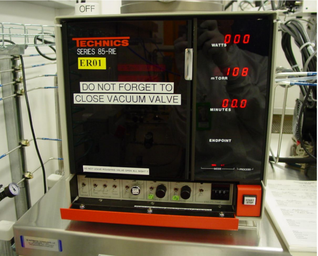
The purpose of the Reactive Ion Etch (RIE) machine is to etch patterns in silicon wafers that have straight walls and a flat bottom. It does this using a gas in plasma state. Since the gas is in plasma form, it is ionized and the individual plasma molecules are then accelerated by an electric field toward the surface of the substrate. Upon striking the surface, they bind with a molecule of the substrate, and then the new electrically neutral molecule floats away. This causes the trench to be evenly etched, with vertical walls and flat floors.
In the world of semiconductor manufacturing, it becomes necessary to etch and remove sections of a wafer of a certain chemical makeup. For example, a person would have to etch a small “hole” into silicon in which to put other materials to make up a transistor. As microchips become faster, more circuit elements must be put on a fixed area of semiconductor material to make up a microchip.
There are several etch methods available to a process engineer. One is a chemical etch, in which resist is lithographically defined on the surface of the substrate in all places except where the etching must actually take place. Then a chemical that dissolves the substrate is applied until the desired depth is reached. The problem with this, however, is that a cross section of the etched hole is not square, but more of a canyon undercutting the resist mask. This can become a problem when a person wishes to etch several holes or lines tightly packed together; those lines will instead form one large line hole with small bumps where straight walls should be.
However, there is a solution to the problem. The RIE Etch tool is capable of digging straight down in areas where the substrate is exposed, causing the resulting holes and lines to have straight, vertical sides.
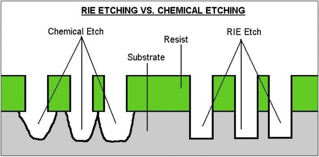
Comparison of Chemical Etch vs. RIE – Notice that the chemical (isotropic) etch is much less precise and can actually damage the resist mask by undercutting it. The RIE (anisotropic etch) is much neater, etching trenches with rectangular cross-sections.
3. Wafer Etching with the RIE Tool
The method described below is a general procedure describing the process of etching wafers with the RIE machine.
-
- Make sure that the machine is free for use and safe to open. You will know it is safe to open the chamber and use the machine if:
- The logbook says “Done” or the finish time is written in.
- There is NOT a sign there saying that it is in use.
- There is NOT a blue glow emanating from the window.
- The POWER switch is off.
- The VAC switch is set to closed.
- The VENT switch may be open or closed. If open, there’s a 99.9% chance its safe.? If you are still not sure, ask someone.
- Sign in to the logbook – fill out the blanks.
- Start preliminary process setup. (Run brief process to stabilize gas flow plasma energy, before submitting your wafer).
- Do not put your wafer in the chamber yet.
- Make sure the VENT is closed.
- The vent allows N2 into the chamber. If the vent and the vacuum were open, the vacuum would simply suck out gas and the vent will let more in, resulting in a waste of time and energy.
- Turn on the VAC switch.
-
- The pressure reading will only display when the vacuum pressure is below 1 Torr, which takes less than 10 seconds to reach.
- If the pressure does not start reading in mTorr in 10 seconds, there’s a problem.
- One possibility may be that the vacuum pump is off. Call a staff member to check out the vacuum system. Chase utilities are off limits to users.
-
- Make sure that the machine is free for use and safe to open. You will know it is safe to open the chamber and use the machine if:
Gas and pump facilities are behind the chase wall and off limits to users.
-
-
- Wait until the pressure gauge reads ~20 mT or less. Then, you are ready to proceed with the setup process.
- Test etch step. Be sure that the MODE switch is set to MANUAL.
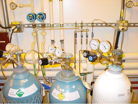
- Open one of the gas valves depending upon what substance you wish to etch:
- Open the O2 gas valve if you are etching PMMA.
- Open the CF4 valve if you are etching silicon.
- The CF4 has 8% oxygen mixed with it, meaning that some of the resist on the surface of the wafer will also be etched away. The oxygen is included to enhance the etch rate of the CF4 into the silicon.
- Open one of the gas valves depending upon what substance you wish to etch:
-
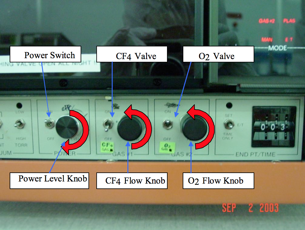
- Adjust the pressure by turning the knob (counterclockwise to increase flow) until the pressure gauge reads the pressure of the gas that you want.
- Higher gas pressure means a faster etch rate up to about 280mT. Increasing pressure above 280mT decreases etch rate and is wasteful.
- You are about to turn on the power.
- Note that higher power means a higher etch rate. However, above 200W, the etch rate it not much higher than the etch rate at 200W. The optimum power value is 200W.
- The longer power is on, the more etching is done. At 200W and 280mT, the etch rate is about 48 angstroms/second for Si.
- Time how long the power is on with a stopwatch or by watching the clock on the wall.
- Turn on the power. You should see a blue glow through the window.
- The blue glow means that etching is happening.
- Turn the power knob to adjust the power level (clockwise to increase).
- The amount of power used in Watts is displayed on the power readout.
- Conclude the test setup.
- To end the etching process, turn the power off.
- Turn off the gas, but do not turn the gas flow knob or power knob. Wait until the pressure dips below ~20mT. Then close the vacuum valve. This removes the poisonous gases from the chamber so that the operator will not be exposed when the lid opens.
- Open the vent valve with the vent switch.
- After a few seconds, you will be able to open the chamber lid.
- Run Wafer Etch Process
1. Place wafer in chamber and close lid.
2. Pump down the chamber and repeat the processes from major Step 2 above. This will assure you that the wafer will see the proper conditions for the full etch time without feeling the effects of adjusting pressure or power variations to set up the process with a wafer in the chamber.
- Conclude by venting the chamber and removing your wafer
- Close the lid and pump down again.
- When the pressure reaches its lower limit, switch off the vacuum line valve. (This prevents back-streaming of oil from the roughing pump over time which contaminates the etch chamber).